In PCB design, multilayer boards, with their sophisticated stack-up structures and complex via technologies, make it possible to achieve highly flexible and nearly “limitless” routing. However, in cost-sensitive designs such as single-layer and double-layer PCBs, as well as in prototyping and post-production rework scenarios, a simple yet clever solution remains indispensable—jumper wires.
In this article, the PCBWay professional design team will detail the role of jumpers in PCB design and how to use them effectively.
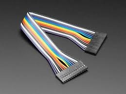
A jumper wire is used to connect two points that would normally be linked through PCB copper traces but cannot be directly routed due to layout constraints.
Its core functions include:
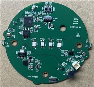
In low-cost double-layer boards, development boards, or PCB rework scenarios, jumper wires serve as a practical and efficient solution.
Simple and low-cost, requiring no PCB redesign. However, manual soldering quality directly impacts reliability, and improper placement may introduce interference or mechanical instability.
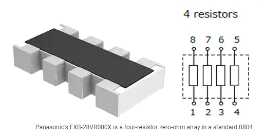
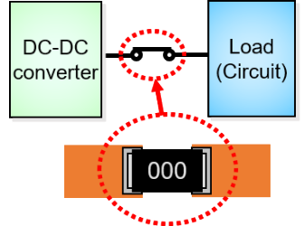
Using zero-ohm resistors as jumpers provides a more stable and manufacturable solution. Proper selection based on current and signal characteristics is essential.
Typically implemented as closely spaced pads that can be shorted with solder, either manually or during reflow. They offer flexibility but require precise soldering control.
Designed as configurable connection points using pin headers and shunts. These are suitable for user-adjustable configurations and mass production scenarios.
In single- or double-layer designs, routing constraints may prevent signal crossover. A jumper (such as a 0Ω resistor or wire) can be inserted to allow one trace to bypass another.
When traces become excessively long or complex, a jumper can serve as a shortcut, reducing routing length and design complexity.
When errors are discovered after fabrication—such as incorrect pin assignments or mislabeled silkscreen—jumper wires (typically hand-soldered) can be used to reroute connections without requiring a board respin, saving both time and cost.
Excessively long or looped jumpers introduce parasitic inductance and resistance, and may increase electromagnetic radiation. Keep jumper paths short and avoid unnecessary loops.
Jumpers should be routed close to the PCB surface and secured using existing pads whenever possible. In environments with vibration or mechanical stress, proper fixation is critical to prevent loosening or breakage.
As uncontrolled conductors, jumpers may introduce crosstalk. Keep them away from high-speed signals, RF traces, and precision analog circuits, and place them in non-critical areas whenever possible.
Ensure that jumper placement does not disrupt the signal return path or reference plane continuity. Minimizing loop area helps reduce EMI and maintain signal integrity.
For mass production, 0Ω resistors are preferred over manual wire jumpers, as they support automated SMT assembly, improve consistency, and simplify debugging and future modifications.
In PCB design, jumper wires play a crucial role in addressing practical layout challenges. They are especially valuable in cost-sensitive, low-layer-count PCB designs, as well as during prototyping or rework stages. Jumper wires provide an efficient and flexible means to overcome routing constraints, shorten redesign cycles, and accelerate development. However, if used improperly, they can cause signal integrity issues, mechanical reliability concerns, and added manufacturing complexity. Therefore, best practice guidelines should be followed to minimize potential drawbacks.
If you need assistance with your PCB design, the PCBWay Design team is ready to help you create your own custom design!